Scanning capacitance microscopy
Scanning capacitance microscopy (SCM) is a variety of scanning probe microscopy in which a narrow probe electrode is held just above the surface of a sample and scanned across the sample. SCM characterizes the surface of the sample using information obtained from the change in electrostatic capacitance between the surface and the probe.
History
SCM was initially devised as a quality control tool for the RCA/CED (Capacitance Electronic Disc),[1] a video disk technology that was a predecessor of the DVD. It has since been adapted for other systems and materials.
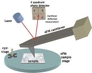
SCM uses an ultra-sharp conducting probe (often Pt/Ir or Co/Cr metal covering an etched silicon probe) to form a metal-insulator-semiconductor (MIS/MOS) capacitor with a semiconductor sample if a native oxide is present. When no oxide is present, a Schottky capacitor is formed. When the probe and surface are in contact, an AC bias is applied, generating capacitance variations in the sample which can be detected using a GHz resonant capacitance sensor. The tip is then scanned across the semiconductor's surface in 2D while the tip's height is controlled by conventional contact force feedback.
By applying an alternating bias to the metal-coated probe, carriers are alternately accumulated and depleted within the semiconductor’s surface layers, changing the tip-sample capacitance. The magnitude of this change in capacitance with the applied voltage gives information about the concentration of carriers (SCM amplitude data), whereas the difference in phase between the capacitance change and the applied, alternating bias carries information about the sign of the charge carriers (SCM phase data). Because SCM functions even through an insulating layer, a finite conductivity is not required to measure the electrical properties.
SCM resolution
On the conducting surfaces, the resolution limit is estimated as 2 nm.[2] For the high resolution, the quick analysis of capacitance of a capacitor with rough electrode is required.[3][4] This SCM resolution is an order of magnitude better than that estimated for the atomic nanoscope; however, as other kinds of the probe microscopy, SCM requires careful preparation of the analyzed surface, which is supposed to be almost flat.
Applications of SCM
Owing to the high spatial resolution of SCM,[2] it is a useful nanospectroscopy characterization tool. Some applications of the SCM technique involve mapping the dopant profile in a semiconductor device on a 10 nm scale,[5] quantification of the local dielectric properties in hafnium-based high-k dielectric films grown by an atomic layer deposition method[6] and the study of the room temperature resonant electronic structure of individual germanium quantum dot with different shapes.[7] The high sensitivity of dynamical scanning capacitance microscopy,[8] in which the capacitance signal is modulated periodically by the tip motion of the atomic force microscope (AFM), was used to image compressible and incompressible strips in a two-dimensional electron gas (2DEG) buried 50 nm below an insulating layer in a large magnetic field and at cryogenic temperatures. [9]
References
- ↑ Matey, JR; J Blanc (1985). "Scanning Capacitance Microscopy". Journal of Applied Physics. 57 (5): 1437–1444. Bibcode:1985JAP....57.1437M. doi:10.1063/1.334506.
- 1 2 Lanyi S; Hruskovic M (2003). "The resolution limit of scanning capacitance microscopes". Journal of Physics D. 36 (5): 598–602. doi:10.1088/0022-3727/36/5/326.
- ↑ N.C.Bruce; A.Garcia-Valenzuela, D.Kouznetsov (2000). "The lateral resolution limit for imaging periodic conducting surfaces in capacitive microscopy". Journal of Physics D. 33 (22): 2890–2898. Bibcode:2000JPhD...33.2890B. doi:10.1088/0022-3727/33/22/305.
- ↑ N.C.Bruce; A.Garcia-Valenzuela, D.Kouznetsov (1999). "Rough-surface capacitor: approximations of the capacitance with elementary functions". Journal of Physics D. 32 (20): 2692–2702. Bibcode:1999JPhD...32.2692B. doi:10.1088/0022-3727/32/20/317.
- ↑ C.C. Williams (1999). "Two-dimensional dopant profiling by scanning capacitance microscopy". Annual Review of Materials Research. 29: 471–504. Bibcode:1999AnRMS..29..471W. doi:10.1146/annurev.matsci.29.1.471.
- ↑ Y. Naitou; A. Ando; H. Ogiso; S. Kamiyama; Y. Nara; K. Nakamura (2005). "Spatial fluctuation of dielectric properties in Hf-based high-k gate films studied by scanning capacitance microscopy". Applied Physics Letters. 87 (25): 252908–1 to 252908–3. Bibcode:2005ApPhL..87y2908N. doi:10.1063/1.2149222.
- ↑ Kin Mun Wong (2009). "Study of the electronic structure of individual free-standing germanium nanodots using spectroscopic scanning capacitance microscopy". Japanese Journal of Applied Physics. 48 (8): 085002–1 to 085002–12. Bibcode:2009JaJAP..48h5002W. doi:10.1143/JJAP.48.085002.
- ↑ A. Baumgartner; M.E. Suddards & C.J. Mellor (2009). "Low-temperature and high magnetic field dynamic scanning capacitance microscope". Review of Scientific Instruments. 80 (1): 013704. arXiv:0812.4146
 . Bibcode:2009RScI...80a3704B. doi:10.1063/1.3069289. PMID 19191438.
 - ↑ M.E. Suddards, A. Baumgartner, M. Henini and C.J. Mellor (2012). "Scanning capacitance imaging of compressible and incompressible quantum Hall effect edge strips". New Journal of Physics. 14: 083015. arXiv:1202.3315. Bibcode:2012NJPh...14h3015S. doi:10.1088/1367-2630/14/8/083015.