SONOS
| Computer memory types |
|---|
| Volatile |
| RAM |
| In development |
| Historical |
|
| Non-volatile |
| ROM |
| NVRAM |
| Early stage NVRAM |
| Mechanical |
| In development |
| Historical |
|
SONOS, short for "Silicon-Oxide-Nitride-Oxide-Silicon", is a type of non-volatile computer memory closely related to Flash RAM. It is one of Charge trap flash variants. It is distinguished from mainstream flash by the use of silicon nitride (Si3N4) instead of polysilicon for the charge storage material. A further variant is "SHINOS" ("Silicon Hi-k Nitride Oxide Silicon"). SONOS promises lower programming voltages and higher program/erase cycle endurance than polysilicon-based flash, and is an area of active research and development effort. Companies offering SONOS-based products include GlobalFoundries, Cypress Semiconductor, Macronix, Toshiba, United Microelectronics Corporation and Floadia .
Description
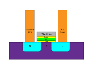
A SONOS memory cell is formed from a standard polysilicon N-channel MOSFET transistor with the addition of a small sliver of silicon nitride inserted inside the transistor's gate oxide. The sliver of nitride is non-conductive but contains a large number of charge trapping sites able to hold an electrostatic charge. The nitride layer is electrically isolated from the surrounding transistor, although charges stored on the nitride directly affect the conductivity of the underlying transistor channel. The oxide/nitride sandwich typically consists of a 2 nm thick oxide lower layer, a 5 nm thick silicon nitride middle layer, and a 5–10 nm oxide upper layer.
When the polysilicon control gate is biased positively, electrons from the transistor source and drain regions tunnel through the oxide layer and get trapped in the silicon nitride. This results in an energy barrier between the drain and the source, raising the threshold voltage Vt (the gate-source voltage necessary for current to flow through the transistor). The electrons can be removed again by applying a negative bias on the control gate.
A SONOS memory array is constructed by fabricating a grid of SONOS transistors which are connected by horizontal and vertical control lines (wordlines and bitlines) to peripheral circuitry such as address decoders and sense amplifiers. After storing or erasing the cell, the controller can measure the state of the cell by passing a small voltage across the source-drain nodes; if current flows the cell must be in the "no trapped electrons" state, which is considered a logical "1". If no current is seen the cell must be in the "trapped electrons" state, which is considered as "0" state. The needed voltages are normally about 2 V for the erased state, and around 4.5 V for the programmed state.
Comparison with standard flash
Generally SONOS is very similar to standard double polysilicon flash, but hypothetically offers higher quality storage. This is due to the smooth homogeneity of the Si3N4 film compared with polycrystalline film which has tiny irregularities. Flash requires the construction of a very high-performance insulating barrier on the gate leads of its transistors, often requiring as many as nine different steps, whereas the oxide layering in SONOS can be more easily produced on existing lines and more easily combined with CMOS logic.
Additionally, traditional flash is less tolerant of oxide defects because a single shorting defect will discharge the entire polysilicon floating gate. The nitride in the SONOS structure is non-conductive, so a short only disturbs a localized patch of charge. Even with the introduction of new insulator technologies this has a definite "lower limit" around 7 to 12 nm, which means it is difficult for flash devices to scale smaller than about 45 nm linewidths. SONOS, on the other hand, requires a very thin layer of insulator in order to work, making the gate area smaller than flash. This allows SONOS to scale to smaller linewidth, with recent examples being produced on 40 nm fabs and claims that it will scale to 20 nm.[1] The linewidth is directly related to the overall storage of the resulting device, and indirectly related to the cost; in theory, SONOS' better scalability will result in higher capacity devices at lower costs.
Additionally, the voltage needed to bias the gate during writing is much smaller than in traditional flash. In order to write flash, power is first built up in a separate device known as a charge pump, which multiplies the input voltage to between 9 V to 20 V. This process takes some time, meaning that writing to a flash cell is much slower than reading, often between 100 and 1000 times slower. The pulse of high power also degrades the cells slightly, meaning that flash devices can only be written to between 10,000 and 100,000 times, depending on the type. SONOS devices require much lower write voltages, typically 5–8 V, and do not degrade in the same way. SONOS does suffer from an unrelated problem, however, where electrons become strongly trapped in the ONO layer and cannot be removed again. Over long usage this can eventually lead to enough trapped electrons to permanently set the cell to the "0" state, similar to the problems in flash. However, in SONOS this requires on the order of a 100 million write cycles, 1000 to 10,000 times better than flash.
History
SONOS was first conceptualized in the 1960s. In the early 1970s initial commercial devices were realized using PMOS transistors and a metal-nitride-oxide (MNOS) stack with a 45 nm nitride storage layer. These devices required up to 30V to operate. By the early 1980s, polysilicon NMOS-based structures were in use with operating voltages under 20 V. By the late 1980s and early 1990s PMOS SONOS structures were demonstrating program/erase voltages in the range of 5–12 volts.[2]
Current efforts
Philips was one of the groups working on SONOS devices,[3] and have produced small 26-bit demonstrators with excellent lifetimes at a 120 nm linewidth. It is not clear if this research is ongoing, however, given the rapid advances in flash technology that have led to very large gains in areal density. Other groups are also working on SONOS for more specialized tasks, notably military and space systems due to its excellent radiation hardness.[4]
In 2007 Spansion announced the development of SONOS flash memory using its MirrorBit technology.[5] Infineon and later its spin-off Qimonda also produced SONOS flash memories.
See also
References
- ↑ Samsung unwraps 40nm "charge trap flash" device // ElectroIQ, 2006-09
- ↑ White, Marvin (July 2000), "On the Go with SONOS", IEEE Circuits & Devices
- ↑ Embedded non-volatile memories (2004)
- ↑ Design Considerations in Scaled SONOS Nonvolatile Memory Devices
- ↑ Spansion || Press Releases